Blogs
Sputtering Targets: Crucial Components in Semiconductor Manufacturing
Introduction
Sputtering targets are indispensable in the realm of semiconductor manufacturing, playing a critical role in the physical vapor deposition (PVD) process to create thin films on substrates. This technique involves high-energy ion bombardment that ejects atoms from the target surface, which then deposit onto a substrate to form a thin layer. The materials used for sputtering targets range from pure metals to complex alloys and compounds, each tailored for specific applications, such as nitride films in reactive sputtering.
Innovations in deposition techniques, including pulsed laser deposition and ion beam-assisted deposition (IBAD), have significantly improved the performance and precision of semiconductor devices. These advancements are crucial in meeting the increasing demands for higher data transfer rates and efficiency in modern electronic applications. As the semiconductor industry continues to evolve, the role of sputtering targets in driving technological progress and innovation remains paramount.
What are Sputtering Targets?
Sputtering materials play an essential role in the physical vapor deposition (PVD) process, vital for forming thin films on substrates in semiconductor manufacturing. In this technique, high-energy ions bombard the surfaces, resulting in the ejection of atoms from the surface which then deposit onto a substrate, forming a thin layer. These targets come in various compositions, including metals, alloys, and compounds, each tailored for specific applications. For instance, reactive sputtering is often employed to create nitride films by introducing a gaseous element from the ion source to react with the evaporated metal. This method has been pivotal in developing substances for optical interference stacks and hard coatings. Furthermore, advancements such as pulsed laser deposition and ion beam-assisted deposition (IBAD) have facilitated the application of intricate multi-compound materials, improving the efficiency of electronic devices. These innovative techniques enable precise control over film composition and structure, satisfying the increasing demand for higher data transfer rates and efficiency in electronic applications.
Applications of Sputtering Targets in Semiconductor Manufacturing
Sputtering materials are essential components in semiconductor manufacturing, utilized in processes such as the deposition of conductive layers, dielectrics, and barrier films. These objectives are crucial for producing integrated circuits, microelectromechanical systems (MEMS), and flat panel displays. The precision of sputtering allows for meticulous control over the thickness and uniformity of the deposited materials, which is vital for the performance and reliability of modern electronic devices.
One notable advancement in sputtering material production is the High-Intensity Vibrational Powder Plating (HIVIPP) method, introduced by Isao Sugai in 1997. This technique was developed to create objectives and foils that are challenging to produce using conventional methods. At Argonne National Laboratory, researchers have successfully employed HIVIPP to fabricate targets of carbon and titanium on various metal backings and are currently exploring its application for other elements, including isotopically enriched and radioactive substances.
The growing electronics sector requires creative methods to keep improving the functionality of integrated circuits. Traditional scaling methods are now complemented by new materials and 3D device architectures. This shift is driven by the need to address sustainability issues such as energy use and greenhouse gas emissions. Plasma etching, for instance, has been pivotal in enabling the production of smaller-scale devices, supporting Moore’s law from micrometer to nanometer dimensions. This method has developed alongside photolithography and thin-film deposition, preserving the economic advantages of the microchip sector.
In the context of organic optoelectronic devices like OLEDs, the arrangement of molecules on thin films is critical. Factors such as deposition rate and surface temperature significantly influence the stability and structure of these films. Recent research from Japan has introduced new deposition methods that optimize molecular arrangement, thereby enhancing device performance.
Overall, the semiconductor industry’s future will be shaped by continuous innovations and the integration of new techniques, ensuring the manufacturing of advanced and sustainable electronic devices.

Key Materials Used in Sputtering Targets
Choosing the suitable substances for sputtering targets is essential, as it greatly influences the characteristics and effectiveness of the resulting films. Common choices include pure metals such as copper and aluminum, alloys like titanium-tungsten, and compounds such as tantalum nitride. High-purity substances are preferred to minimize contamination and maintain the integrity of deposited films, which is essential for device functionality. Advanced techniques like pulsed laser deposition can further enhance performance by enabling the deposition of complex multi-compound substances, including high concentrations of scandium in aluminum scandium nitride films. This method, although previously limited to laboratory scales, is gaining traction in high-volume manufacturing due to its ability to address technical challenges such as film uniformity and particle filtering. The growing demand for higher data transfer rates in wireless technologies underscores the importance of these advancements. As noted by industry leaders, the role of material selection in manufacturing cannot be overstated, as it directly impacts the success of the final product.
The Sputtering Process in IC Fabrication
In the sputtering process for integrated circuit fabrication, a vacuum environment is essential. Argon, an inert gas, is introduced, and a high voltage is applied to create a plasma that ionizes the gas. The resulting ions collide with the sputtering target, dislodging atoms that then travel to the substrate. This technique enables accurate management of deposition rates and consistency, essential for high-performance electronic devices. This technique is becoming even more vital as manufacturers, like Samsung, invest billions in advanced facilities to push the boundaries of technology, aiming for innovations such as 3-nanometer process technology.

Importance of High-Purity Sputtering Targets
High-purity sputtering targets are essential in preserving the integrity and performance of electronic components. Impurities can introduce defects in the deposited films, which subsequently impacts electrical properties and device reliability. As the microchip sector progresses, the need for greater purity standards increases. According to recent industry trends, the need for advanced materials and technologies such as silicon carbide (SiC) and gallium nitride (Gan) is growing due to their superior properties compared to traditional silicon. This shift is driven by their enhanced dielectric breakdown field strength, mobility, and thermal conductivity, which are crucial for power semiconductors.
Manufacturers are increasingly adopting stringent quality control measures in focused production to meet these elevated purity standards. For instance, Argonne National Laboratory’s innovative HIVIPP method has enabled the production of high-purity targets that were previously challenging to manufacture. This advancement highlights the critical role of continuous innovation in addressing the changing needs of the technology sector.
Moreover, the worldwide growth of chip manufacturing plants, backed by significant government funding, underscores the sector’s dedication to enhancing production capacity. This expansion is essential to prevent global competition gaps and ensure the steady supply of high-quality sputtering materials.
In conclusion, the relentless pursuit of higher purity levels in sputtering materials is a testament to the industry’s dedication to advancing electronic technology. This commitment not only enhances device performance but also supports the broader goal of technological innovation and market growth.
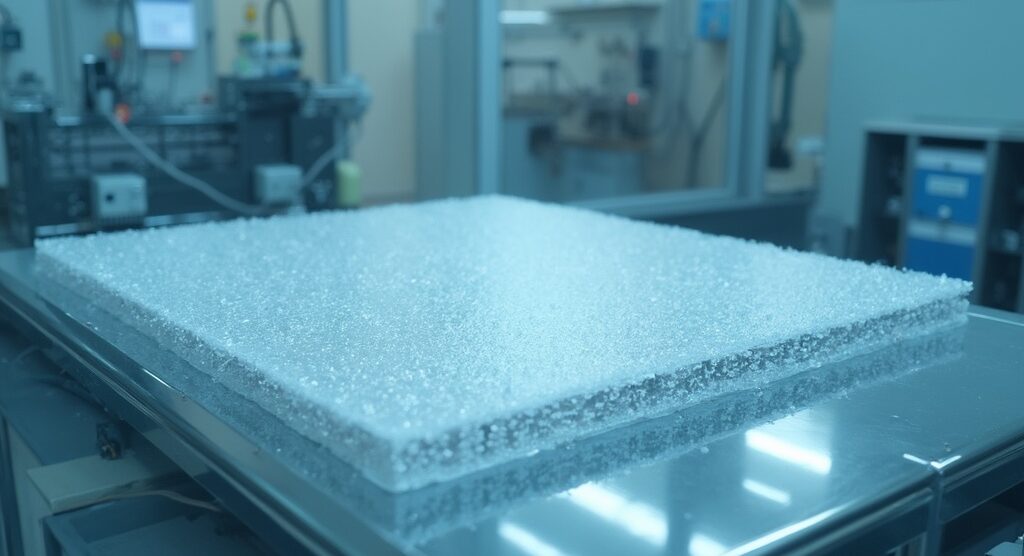
Sputtering Target Manufacturing Process
‘The manufacturing process for sputtering materials is a meticulous and multi-step procedure that ensures the highest quality for semiconductor fabrication.’. It begins with the careful selection of high-purity substances such as silicon carbide (SiC), indium phosphide (InP), and gallium nitride (Gan), which are essential for their high-temperature resistance and reduced brittleness under irradiation. These raw materials are then processed to form intended blanks through sintering at elevated temperatures, a crucial step to achieve the desired density and structural integrity.
After sintering, the blanks undergo precision machining to meet stringent dimensional and surface quality specifications. This stage is essential, as even minor deviations can affect the performance and reliability of the sputtering materials in advanced applications such as electronics, medical devices, and aerospace engineering. The accuracy needed in machining is similar to that in the co-development processes in other sectors, where ongoing feedback and iteration between design engineers and manufacturers result in higher quality products.
Incorporating automated single-wafer systems like JST Manufacturing’s Ospray tools can further enhance the manufacturing process. These systems offer high-uniformity surface preparation and superior repeatability, essential for handling complex and fragile substrates. ‘The incorporation of such cutting-edge technologies guarantees that the sputtering materials satisfy the changing requirements of the microelectronics sector, facilitating a smooth and effective manufacturing process.’.

Challenges and Future Trends in Sputtering Targets
The sputtering target industry is navigating significant challenges, including escalating raw resource costs and an increasing demand for sustainable practices. As technology in the field continues to progress, there is an increased focus on creating substances and methods that not only improve efficiency but also reduce ecological effects. For instance, Morgan Advanced Materials underscores the importance of using advanced materials to tackle complex problems while improving resource efficiency and life quality.
Future trends in the sector may include incorporating advanced alloys and composites to meet the high-performance demands of modern semiconductors. Additionally, innovations in target recycling and reuse are essential for achieving sustainability goals. Vetter’s recent efforts in integrating a comprehensive sustainability management system, powered by 1,700 photovoltaic modules, exemplify the industry’s move towards more eco-friendly operations.
Governments globally are also contributing by injecting substantial funds to establish new chip manufacturing facilities. This investment aims to boost production capacity and maintain global competitiveness. As China leads in developing chip production facilities, the global market is expected to see significant growth in the need for new equipment, including silicon and test and measurement tools.
The shift towards electric vehicles (EVs) has further amplified the demand for electronic components, particularly for enhancing battery voltage to meet the consumer demand for faster charging. This shift necessitates increased investment in test and measurement equipment to ensure safety and reliability. As the semiconductor industry rebounds from previous supply chain disruptions, a cautious yet optimistic growth trajectory is anticipated.

Conclusion
Sputtering targets are integral to semiconductor manufacturing, serving as the foundation for thin film deposition processes that are vital for creating advanced electronic devices. The importance of high-purity materials and innovative techniques cannot be overstated, as they directly influence the performance and reliability of the final products. With the continuous evolution of materials such as silicon carbide and gallium nitride, the semiconductor industry is poised to meet rising demands for efficiency and data transfer rates.
Challenges such as escalating raw material costs and the need for sustainable practices are driving the industry towards innovative solutions. The adoption of advanced alloys, composites, and recycling initiatives reflects a commitment to both performance enhancement and environmental stewardship. Additionally, significant governmental investments in semiconductor fabrication facilities underscore the urgency to bolster production capabilities and maintain competitive advantage on a global scale.
Looking ahead, the future of sputtering targets will be shaped by ongoing technological advancements and a strategic focus on sustainability. As the demand for semiconductors, particularly in emerging sectors like electric vehicles, continues to rise, the industry will need to adapt and innovate. The relentless pursuit of excellence in sputtering target manufacturing not only supports technological innovation but also ensures the sustainable growth of the semiconductor landscape.