Blogs
Sputtering Targets Performance: 7 Powerful Reasons UNS C10100 Defines High-Performance Thin Films | DOMADIA™
Sputtering Targets Performance Starts Where Most Engineers Stop Looking
Sputtering Targets Performance is rarely the first thing discussed in thin-film meetings.
Process parameters get attention. Vacuum levels are debated. Power density is optimized.
And yet, across semiconductor fabs, optical coating lines, and advanced electronics plants, one silent factor keeps deciding success or failure—the sputtering target itself.
A fabrication manager once shared how two identical sputtering systems produced completely different film adhesion results. Same chamber. Same gas flow. Same power.
The only difference? The purity and microstructure of the sputtering target.
That moment changed how their team approached thin-film reliability.
This is where Sputtering Targets Performance becomes the hidden differentiator.
What Are Sputtering Targets? (And Why They Matter More Than You Think)
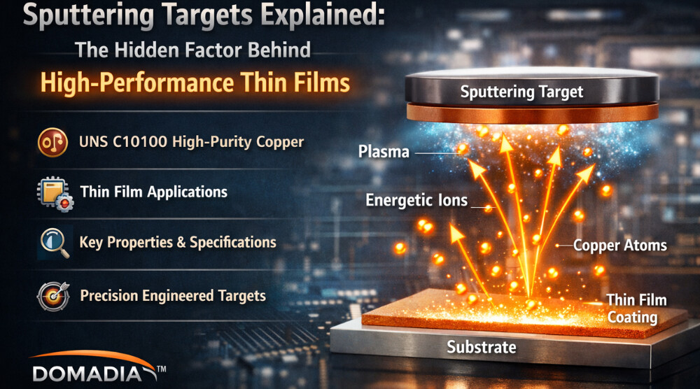
A sputtering target is the source material used in physical vapor deposition (PVD). Under plasma bombardment, atoms eject from the target surface and deposit as ultra-thin, uniform films.
Every characteristic of the target transfers directly into the film:
- Purity
- Grain structure
- Density
- Chemical consistency
For copper thin films, UNS C10100 (Oxygen-Free Electronic Copper) has become a preferred choice for applications where conductivity, adhesion, and defect control are non-negotiable.
Mindset Shift: Thin-Film Failures Are Rarely Process Problems
Most production teams treat film defects as tuning issues.
The reality is harsher.
When Sputtering Targets Performance is compromised, no amount of parameter optimization can fix:
- Particle generation
- Micro-arcing
- Non-uniform thickness
- Poor step coverage
- Film contamination
High-performance thin films start with material discipline, not just equipment precision.
Chemical Composition of UNS C10100 Sputtering Targets
DOMADIA™ supplies sputtering targets manufactured from UNS C10100, known for its ultra-high purity.
Typical Composition:
- Copper (Cu): ≥ 99.99%
- Oxygen: ≤ 0.0005%
- Residual elements: Controlled to trace levels
This purity ensures:
- Stable plasma behavior
- Minimal particle shedding
- Superior electrical conductivity in deposited films
Key Properties That Define Sputtering Targets Performance
Electrical Properties
- Electrical Conductivity: ~101% IACS
- Low resistivity ensures efficient energy transfer during sputtering
Thermal Properties
- High thermal conductivity enables better heat dissipation
- Reduced target cracking under high-power sputtering
Mechanical Properties
- Dense microstructure
- Low porosity minimizes arcing and film defects
Chemical Stability
- Oxygen-free composition prevents oxide-related contamination
- Clean film interfaces for advanced electronics
Technical Specifications (Typical for DOMADIA™ Targets)
| Parameter | Specification |
| UNS Number | C10100 |
| Purity | 99.99% min |
| Density | ≥ 99.9% theoretical |
| Grain Structure | Fine & uniform |
| Oxygen Content | ≤ 5 ppm |
| Bonding | Indium or elastomer bonded |
| Backing Plate | Copper / Stainless Steel |
Shapes Available for Sputtering Targets
DOMADIA™ offers sputtering targets engineered for system compatibility:
- Circular Disc Targets
- Rectangular & Planar Targets
- Cylindrical & Rotatable Targets
- Custom geometries for OEM chambers
Precision machining ensures optimal erosion profiles and extended target life.
Applications Where Sputtering Targets Performance Is Mission-Critical

Semiconductor Interconnects
Sputtering Targets Performance plays a critical role in copper thin films used in IC interconnects, where ultra-low defect density is essential to prevent signal loss and electromigration failures. High-purity sputtering targets enhance Sputtering Targets Performance by ensuring uniform grain growth, reliable line conductivity, and long-term device reliability at nanometer scales.
Display & Touch Panels
Transparent conductive layers in displays and touch panels depend on stable sputtering behavior for uniform thickness and optical clarity. Inconsistent target composition can lead to haze, pixel defects, and reduced panel lifespan.
Solar Cells
High-purity copper layers improve charge collection efficiency and reduce resistive losses in solar cells. Consistent sputtering targets help maintain film adhesion and electrical stability over prolonged outdoor thermal cycling.
MEMS & Sensors
MEMS devices and precision sensors rely on thin films with controlled composition for accurate signal response. Even minor contamination from sputtering targets can alter sensitivity, drift performance, and calibration stability.
Advanced Electronics & EV Systems
Power electronics and EV components experience repeated thermal cycling and high current loads. Flawless thin-film deposition using stable sputtering targets ensures durability, conductivity, and failure resistance under demanding operating conditions.
Standards Followed
DOMADIA™ sputtering targets align with:
- ASTM B170 / B187 (Copper specifications)
- SEMI material purity guidelines
- Customer-specific semiconductor standards
Compliance ensures reproducibility across global fabrication lines.
Actionable Fix: How to Improve Thin-Film Yield Immediately
If yield losses persist:
- Audit target purity, not just chamber parameters
- Inspect grain structure and density reports
- Replace recycled or mixed-grade targets
- Match target metallurgy to power density
- Work with suppliers who control raw material sourcing
This single shift often improves uptime faster than equipment upgrades.
Why DOMADIA™ for High-Performance Sputtering Targets
DOMADIA™ focuses on material integrity first:
- Controlled melting and casting
- Strict purity verification
- Consistent grain refinement
- Custom machining with tight tolerances
Because in thin-film engineering, material shortcuts always surface later—as downtime.
Conclusion: Sputtering Targets Performance Is the Foundation of Thin Films
Sputtering Targets Performance determines whether thin films succeed quietly—or fail expensively.
When purity, structure, and consistency align, process stability follows naturally.
For advanced coatings, electronics, and semiconductor reliability, the target is never just a consumable—it is the process foundation.
Reduce particle defects, stabilize plasma behavior, and improve thin-film yield with precision-engineered sputtering targets.
For expert guidance on high-performance sputtering targets that improve film quality and process uptime, Contact usand speak with DOMADIA™ specialists.
Talk to: Er.Pankaj Domadia | Kairav Domadia | Aadil Domadia | Pragati Sanap | Pooja N N
#SputteringTargetsPerformance #ThinFilmTechnology #UNSC10100 #PVDCoatings #DOMADIA #SemiconductorMaterials
Directly whatsapp us for an Enquiry: https://wa.link/kairav
We’ve supplied to Mumbai, Pune, Indore, Jaipur, and Surat—serving industries across Maharashtra, Madhya Pradesh, Rajasthan, Gujarat, and Goa, with exports to Germany, USA, Japan, South Korea, and Italy.

