Blogs
Understanding Sputtering Targets for Semiconductor Fabrication: An In-Depth Tutorial
Introduction
In the intricate landscape of semiconductor manufacturing, sputtering targets emerge as pivotal components, shaping the efficiency and performance of advanced electronic devices. These materials, essential for the physical vapor deposition process, enable the creation of high-quality thin films that are fundamental to a myriad of applications, from integrated circuits to optical coatings.
With substantial investments in semiconductor R&D—such as the staggering USD 124 billion allocated by the U.S. in 2021—understanding the nuances of sputtering targets has never been more critical for procurement managers.
As the market evolves, characterized by a shift towards advanced materials and a heightened focus on sustainability, the strategic selection of sputtering targets will play a decisive role in maintaining competitive advantage in this rapidly advancing field.
This article delves into the definition, types, manufacturing processes, applications, and future trends of sputtering targets, providing valuable insights for informed decision-making in procurement strategies.
Introduction to Sputtering Targets: Definition and Importance
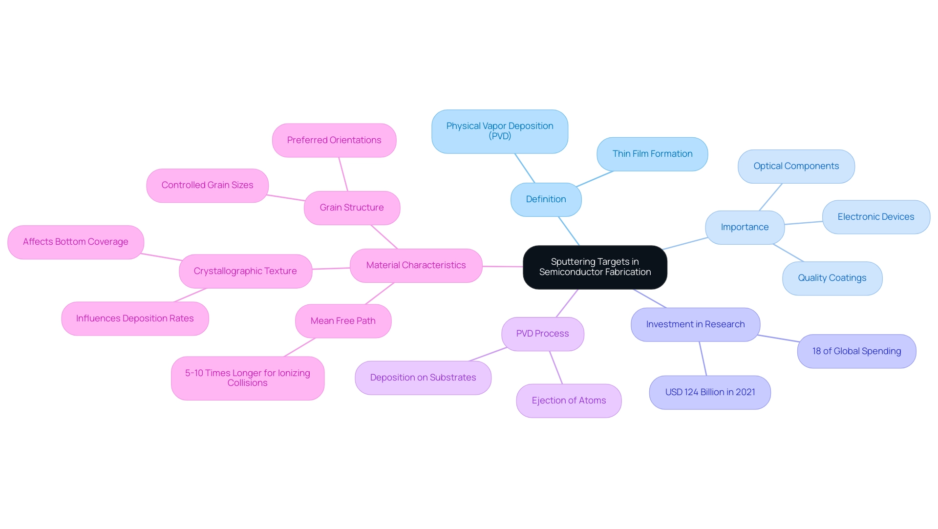
Sputtering targets for semiconductor fabrication are vital materials in the physical vapor deposition (PVD) process, where atoms are ejected from a solid substance and meticulously deposited onto substrates to form thin films. These materials are essential for producing high-quality coatings that are vital in electronic devices, optical components, and a wide range of electronic applications. The importance of target materials is highlighted by the considerable investment in chip research and development, with the U.S. alone designating USD 124 billion in 2021, representing roughly 18% of worldwide expenditure.
Such investments emphasize the critical need for advanced materials and sputtering targets for semiconductor fabrication techniques in semiconductor manufacturing. Furthermore, it is crucial to highlight that the mean free path to an ionizing collision is 5–10 times longer than the mean free path to any collision, a detail that is pertinent to comprehending the ejection process and its efficiency. Recent modeling studies further indicate that the crystallographic texture of deposition materials significantly affects rates of deposition and bottom coverage, illustrating the intricate relationship between material characteristics and end-product quality.
As procurement managers, understanding the intricacies of sputtering targets for semiconductor fabrication is crucial, as their selection and quality directly influence the performance and reliability of electronic products. This knowledge is further supported by the National Institute of Standards and Technology (NIST), which established a new Semiconductor Metrology Division in December 2023 to enhance measurement techniques crucial for this sector. Moreover, case studies focusing on grain structure reveal that controlled grain sizes and orientations are preferred, as they improve sputtering rates and ensure uniform deposition, thereby enhancing material properties.
Advanced processing techniques, such as powder metallurgy and controlled cooling, are employed to optimize grain structure, ensuring consistent deposition rates and improved material properties. Such insights are invaluable for making informed procurement decisions in the rapidly evolving technology landscape.
Types of Sputtering Targets: Materials and Applications
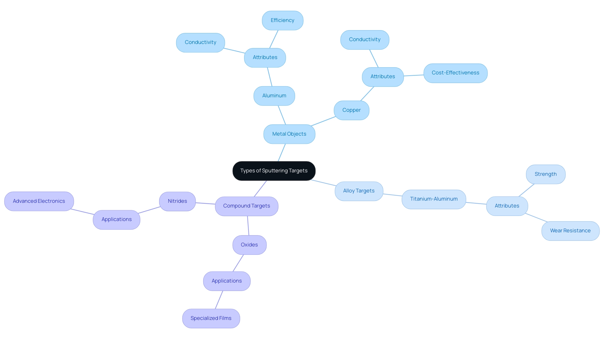
Sputtering materials can be classified into three primary categories, each offering unique attributes and applications critical to semiconductor fabrication:
- Metal Objects: These items are essential for producing conductive films, with aluminum and copper being the most prevalent choices. They are widely recognized for their efficiency and effectiveness in various electronic applications.
- Alloy Targets: Composed of metal mixtures such as titanium and aluminum, alloy targets enhance performance by improving specific properties, including strength and wear resistance. Their adaptability makes them appropriate for a variety of electronic manufacturing techniques.
- Compound Targets: This category includes materials like oxides and nitrides, which are specifically formulated for use in advanced electronic applications. Their unique chemical properties enable the creation of specialized films that meet stringent performance requirements.
Comprehending these types and their respective roles in semiconductor operations, especially sputtering targets for semiconductor fabrication, is essential for procurement managers, as it enables informed decision-making that aligns with the latest market trends and technological advancements.
The Sputtering Targets Market is segmented based on type, application, and geography. With the market valued at USD 3.85 billion in 2022 and projected to reach USD 5.60 billion by 2030—reflecting a robust growth trajectory—the market is expected to grow at a CAGR of 0.7% from 2023 to 2033. Understanding the applications and advantages of each category type is essential for strategic sourcing.
Manufacturing Processes of Sputtering Targets: Techniques and Quality Control
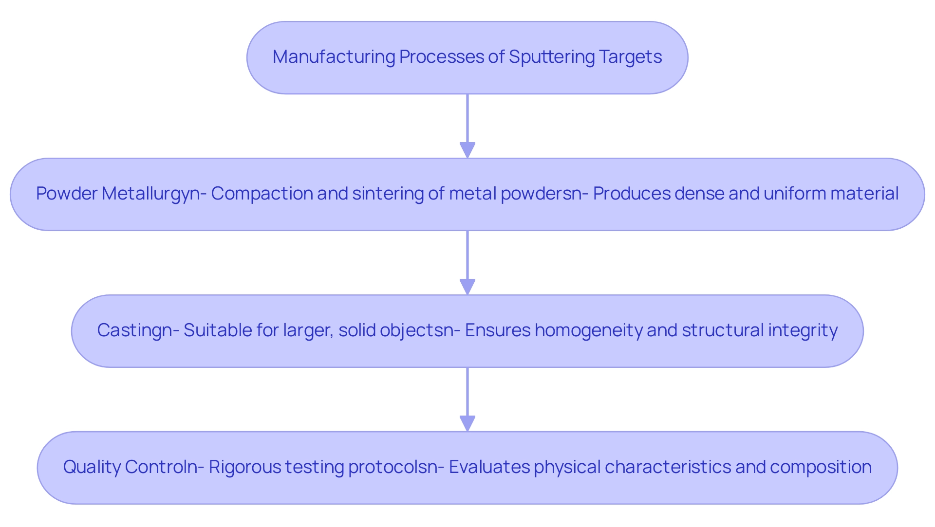
The production of sputtering materials involves several crucial steps that are vital for guaranteeing product quality and performance. These processes include:
Powder Metallurgy: This widely utilized method is essential for producing metal and alloy targets. It involves the compaction and sintering of metal powders, resulting in a dense and uniform material that meets specific requirements.
Casting: Particularly suited for larger, solid objects, casting ensures both homogeneity and structural integrity. This method is essential for applications where uniformity of the objective is critical for consistent deposition results.
Quality Control: Rigorous testing protocols are implemented throughout the manufacturing process. This encompasses thorough evaluations of physical characteristics, such as density and thermal conductivity, along with compositional analyses to confirm that each item complies with stringent industry standards.
Understanding these manufacturing techniques is imperative for procurement managers aiming to source high-quality sputtering targets. As the market is projected to grow at a CAGR of 0.7% to reach USD 6,200 million by 2033, Europe is anticipated to be a key growth market due to its expanding electronics industry and government support for renewable energy.
These insights allow for informed decision-making in a competitive landscape. Verified Market Research emphasizes,
This way, we ensure that all our clients get reliable insights associated with the market,
further underlining the importance of quality assurance in manufacturing practices. Furthermore, North America is notable as an important area for coating materials, propelled by strong research and development efforts and the presence of leading chip producers.
These processes together support the reliability and effectiveness of sputtering targets for semiconductor fabrication in electronic applications.
Applications of Sputtering Targets in Semiconductor Manufacturing
Sputtering targets for semiconductor fabrication are essential materials for a broad range of chip fabrication processes. Their critical roles include:
- Integrated Circuits (ICs): Sputtering targets are essential for depositing conductive layers, which are fundamental to the functionality of microelectronics. As chip technology progresses, the precision and quality of these layers become increasingly important, particularly for technology nodes below 110 nm. The substantial U.S. investment of USD 124 billion in semiconductor research and development in 2021 emphasizes the industry’s emphasis on improving these technologies, underscoring the significance of high-quality deposition materials in realizing these advancements.
- Solar Cells: In the field of renewable energy, deposition materials are essential for the creation of thin-film photovoltaic cells, which improve energy conversion efficiency. The increasing need for sustainable energy options is fueling creativity in this field, making the efficient procurement of high-quality materials essential.
- Optical Coatings: These targets are employed in the application of coatings for lenses and mirrors, significantly improving performance characteristics. The need for optical parts in different sectors highlights the importance of dependable deposition methods.
Recent investments underscore the industry’s dedication to advancing these technologies, with the U.S. alone investing USD 124 billion in research and development in 2021, representing approximately 18% of global expenditure in this sector. Additionally, the National Institute of Standards and Technology (NIST) created a new Metrology Division for electronic components in December 2023 to aid progress in measurement methods for microchip production, highlighting the significance of accurate deposition techniques. Based on the case study named “Future Trends in Usage of Deposition Materials,” as wafer production methods advance, the need for copper, tantalum, and titanium materials is anticipated to rise, mirroring the sector’s requirement for improved performance and efficiency in microchip manufacturing.
Understanding these applications enables procurement managers to effectively align their sourcing strategies with the evolving needs of the industry, ensuring they remain competitive in a rapidly advancing field.
Market Trends and Future Outlook for Sputtering Targets
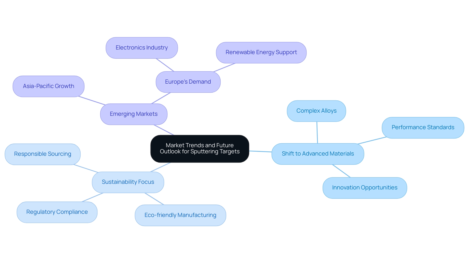
The fluctuating materials market is presently undergoing a major change, propelled by progress in chip technology and shifting industry demands. Key trends shaping this landscape include:
Shift to Advanced Materials: There is a marked increase in the utilization of complex alloys and compounds, which are essential for meeting the stringent performance standards demanded by modern semiconductor applications. This change not only improves the efficiency of deposition materials but also creates opportunities for innovation in material science.
Sustainability Focus: As industries become increasingly aware of their environmental impact, the emphasis on responsible sourcing of materials and the adoption of eco-friendly manufacturing practices has intensified. Manufacturers are prioritizing sustainability in their operations to align with both regulatory expectations and consumer preferences, thereby fostering a competitive edge in the market.
Emerging Markets: The Asia-Pacific region is poised for substantial growth, propelled by the rising electronics production and government support for renewable energy initiatives. This market growth is backed by a well-established infrastructure and technological foundation, creating opportunities for heightened demand for deposition materials. For instance, Europe’s increasing need for coating materials is reflective of this trend, propelled by the expanding electronics sector and governmental backing for renewable energy.
Regarding market analysis, the Coating Materials Market Report CMR 2024-2025 is priced at $8,900.00, emphasizing the worth of insights available for procurement managers. Looking ahead, the market for sputtering targets for semiconductor fabrication is forecasted to exhibit robust growth, presenting numerous opportunities for strategic sourcing and partnerships. Verified Market Reports suggests that as industries are predominantly shaped by technological advancements, consumer preferences, and regulatory changes, procurement managers should remain vigilant to capitalize on these trends to enhance their sourcing strategies.
Conclusion
The exploration of sputtering targets within semiconductor manufacturing reveals their indispensable role in producing advanced electronic devices. From the fundamental processes of physical vapor deposition to the diverse types of targets—metal, alloy, and compound—each category offers unique advantages essential for various applications. The insights into manufacturing techniques, such as powder metallurgy and casting, underscore the importance of quality control in ensuring optimal performance and reliability.
As technology evolves, the applications of sputtering targets in integrated circuits, solar cells, and optical coatings highlight their critical function in driving innovation. The substantial investments in semiconductor R&D, particularly in the U.S., reflect the industry’s commitment to enhancing these technologies. With the market projected for continuous growth, understanding current trends—such as the shift towards advanced materials and sustainability—will be crucial for procurement managers aiming to maintain a competitive edge.
In an era where precision and quality are paramount, the strategic selection of sputtering targets becomes not just a procurement decision but a vital component of overall manufacturing success. As the landscape evolves, staying informed about the latest developments and market dynamics will empower procurement professionals to make educated choices that align with the future of semiconductor manufacturing. Embracing these insights will facilitate a proactive approach to sourcing, ensuring the delivery of high-quality products that meet the demands of a rapidly advancing industry.


